
深圳PCB厂家打样周期一般是多久?
Views : 2629
Update time : 2016-11-12 11:10:00
随着互联网的到来,客户对PCB板打样的交期也发生了变化,那么PCB线路板打样周期到底要多久呢?关于这个问题,只能大致介绍(原因是每个PCB厂的条件及设备都不一样,打样时间也有所差别),深圳亚恒电路有限公司PCB打样周期为:
单面PCB打样交期:正常交期2~3天,可12、24小时加急
双面PCB板打样交期:正常交期2~3天,可12、24小时加急
四层线路板打样交期:正常交期4~5天,可12、24、72小时加急
六层电路板打样交期:正常交期6~7天,可72小时加急
led铝基板打样交期:正常交期3~4天,可72小时加急
PCB线路板小批量打样交期:5平米内5~6天;10平米内6~7天;10平米以上8~9天
温馨提示:
1、除了亚光黑,亚光绿和紫色,其它颜色,我们一律免费!
2、当天18点前下单付款,PCB打样交期从第二天开始计算
3、线路板打样12小时加急:上午11:00前下单付款,交期为当天晚上23:00发货,下午17:30前下单付款,交期为第二天上午12:00前发货
4、以上时间是指PCB线路板工厂交货时间,物流时间另计。
相关新闻
 Circuit Board Assembly Services for OEM Plant Production
Aug .02.2018
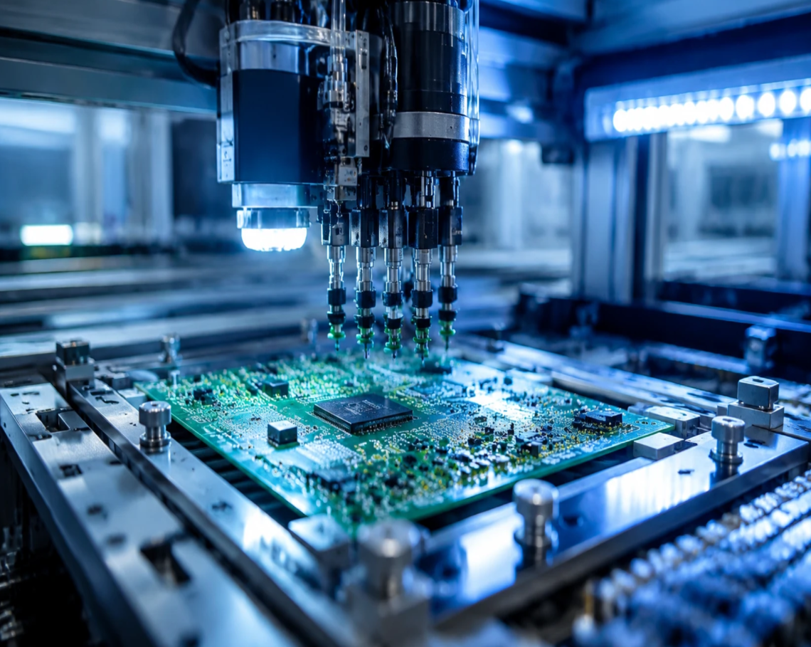
In the modern industrial manufacturing ecosystem, electronic hardware reliability directly determines brand reputation, operational uptime, and total product lifecycle costs. Whether engineering high-frequency power controllers, automotive ECU modules, automated robotics gear, or IoT smart grid sensors, original equipment manufacturers (OEMs) face increasing pressure to balance miniaturization with thermal stability and mechanical robustness. At the center of this engineering push sits high-precision circuit board assembly.
 How PCB vias impact the signal transmission
Aug .02.2018
Via is one of the most important parts of multilayer PCB board. The drilling cost usually accounts for 30% to 40% of PCB board cost.Simply put, every hole in the PCB can be called a through hole.
 Why choose Yaheng Circuits as your China PCB supplier?
Aug .02.2018
There are at least 7 reasons you buy from us the in the following:
Real factory not broker, Cost saving and will never sacrifice the quality, Quality control,No time difference, Convenient tansporation and logistic service.
 The Advantages and applications of PCB multilayer circuit boards
Aug .02.2018
As the name suggests, a multi-layer circuit board can be called a multi-layer circuit board with more than two layers, such as four layers, six layers, eight layers and so on. Of course, some designs are three-layer or five-layer circuits, also called multi-layer PCB circuit boards.
